Business
Business Overview

Materials/Components

SILICON
Silicon parts for semiconductor applications are primarily used as consumable components within the chambers of etching processes. In recent years, as semiconductor manufacturing has advanced toward higher performance and finer patterning, the proportion of silicon part usage has continued to increase.
With their high heat and plasma resistance and lower contamination compared to metal materials, silicon parts protect the interior of equipment from plasma and chemical reactions and play an essential role in preventing process contamination.
Our Production and Sales System


CMTX maintains a stable supply of silicon ingots from its subsidiary SELIG and supplies a wide range of silicon parts to customers in Korea and around the world, continually expanding its reach across the global market.
Silicon Material Properties
| Single-Crystal Silicon | Polycrystalline Silicon | |
|---|---|---|
| Crystal Structure | Single crystal | Polycrystalline |
| Density | Approx. 2.329 g/cm³ | Approx. 2.32~2.33 g/cm³ |
| Thermal Conductivity | Approx. 149 W/m·K | Approx. 80~120 W/m·K |
| Bandgap | Approx. 1.12 eV (300K) | Approx. 1.12 eV (identical, though with more crystal defects) |
| Specific Heat | Approx. 700 J/kg·K | Approx. 700 J/kg·K |
| Thermal Expansion Coefficient | 2.6 × 10⁻⁶ /K | Approx. 2.5~2.7 × 10⁻⁶ /K |
| Electrical Resistivity | 10⁴~10⁶ Ω·cm | 10⁴~10⁶ Ω·cm |
| Mechanical Strength | Approx. 7000 MPa (tensile strength varies by crystal orientation) | Lower overall (200~400 MPa) |
CMTX produces both single-crystal and polycrystalline silicon internally, delivering a fully integrated one-stop solution that ensures tailored customer support, consistent product quality, reliable lead times, and robust technical assistance.
Main Products
| Equipment | Purpose |
|---|---|
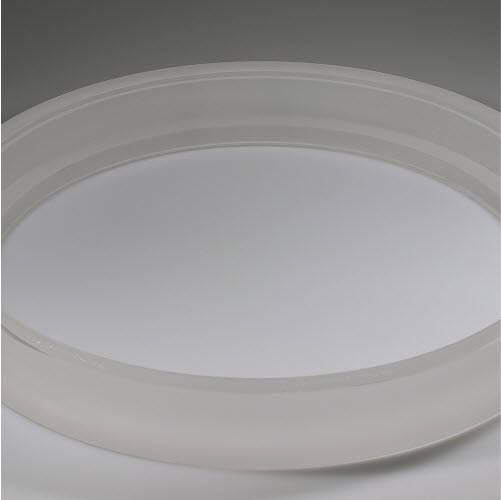
| Silicon C-Shroud Ring Silicon Outer Ring |
Protects the wafer edge inside the chamber to enhance wafer yield. These components also stabilize gas flow and plasma regions within the chamber, serving to block and minimize particle generation. |
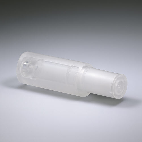
| Silicon Electrode | Functions as both a plasma generator and wafer support, while promoting uniform plasma distribution across the chamber. |
| Silicon Curved Electrode | Featuring a convex or concave design rather than a flat surface, this electrode is optimized for precise control of electric field distribution and plasma density. |