R&D
R&D

Achievements and Activities
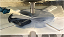
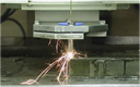
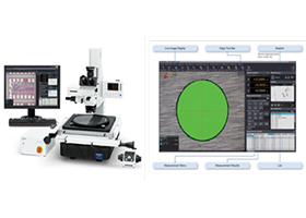
Hole Technology
| Hole Machining Method | Process window | |||||
|---|---|---|---|---|---|---|
| PCD | EDM | Hole size (mm) |
Cross-Section Machining Standard (Single-sided ) | Aspect ratio (Depth / Hole) |
Finished Product Standard (Product) |
|
| Mass-production | R&D | |||||
| Max. Depth (mm) | Max. Depth (mm) | |||||
 |
 |
0.30 | 6.5 | 7.5 | 21.7 | 12T |
| 0.35 | 7.7 | 9.0 | 22.0 | 12T | ||
| 0.40 | 9.0 | 10.5 | 22.5 | 18T | ||
| 0.50 | 12.0 | 15.0 | 24.0 | 24T | ||
| 0.80 | 24.0 | 30.0 | 30.0 | 24T < | ||
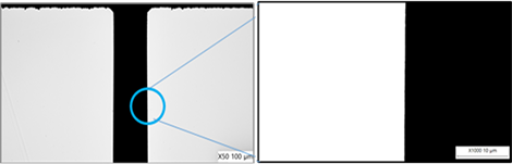
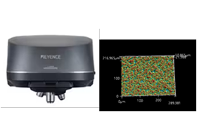
| Hole Image | Before Precision Chemical Etching | After Precision Chemical Etching |
|---|---|---|
 |
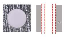 |
Precision Chemical Etching’s Effect on Hole Side
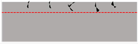
DoD (Depth of Damage)
< Removing the damage layer >
Surface Technology
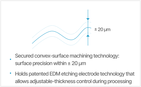
Curved / Shaped machining

Key point
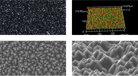
Surface etching Technology
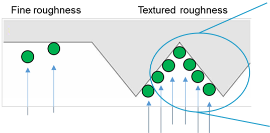
Texturing surface
F/A(Failure Analysis)
Operation of analysis laboratory (material property analysis, consumable wear measurement, defect analysis)
Scope

FTIR
Laser microscope
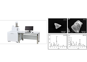
SEM / EDX
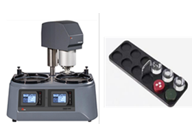
Sample Polisher
ICP-MS
UTM
| Category | Major Equipment | Analysis Items | Application Purpose |
|---|---|---|---|
| Surface Analysis | SEM, Laser Scope | Microstructure, surface roughness, chemical bonding states | Assessment of surface morphology and composition |
| Material Property Analysis | UTM | Material Property Analysis UTM Mechanical properties (strength, tensile, compression) | Verification of material properties and quality control |
| Composition Analysis | EDS, FT-IR | Elemental makeup, molecular structure, impurities | Identification of chemical and elemental composition |
| Purity Analysis | ICP-MS | Ultra-trace element quantification, impurity analysis | Analysis of high-purity materials |
Machining Simulation
-
1. Machining Safety & Reliability Verification
Prevents potential collisions, interferences, and operational errors through pre-simulation.
Validates every machining element from equipment to tooling within a virtual environment.
-
2. Process Optimization & Cost Reduction
Reviews and shortens tool paths and machining time to enhance production efficiency.
Allows machinability analysis without the need for prototypes.
Reduces losses caused by equipment malfunction or tool damage.
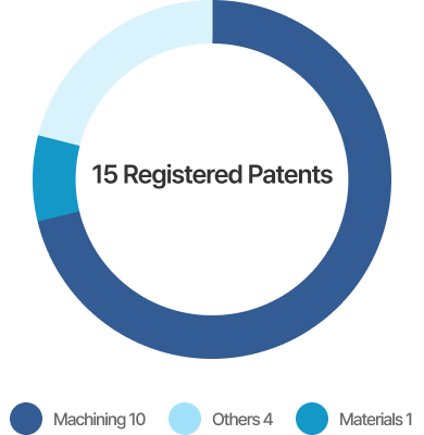
Patent Portfolio
Research Achievements
- Etching and micro-crack removal technologies (patented, independently developed)
- Advanced precision etching and EDM technologies
- Vertical pressurized etching device and process-control technology for micro-hole machining in semiconductor cathodes
- Etching upper electrode featuring curved surfaces and variable thickness using EDM electrodes
- Sapphire-based high-durability component manufacturing technology (for CVD processes)
- Production capability for monocrystalline silicon ingot materials used in silicon parts (patented)
Projects / Certifications

Designated as a Gyeongbuk PRIDE Company
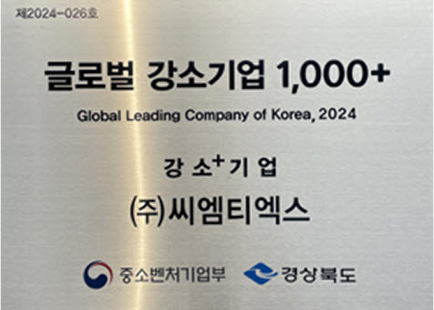
Designated as one of the 1,000+ Global Strong SMEs

Selected for the Jump-Up Program